Back To Thought Leadership

How to Improve FPGA Data Throughput? Integrated Optical Transceivers
Published: 01/20/26
Published: 01/20/26
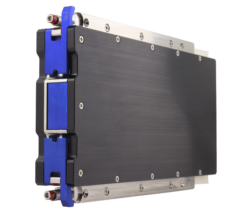
FPGAs are on the verge of a major shift: rugged optical transceivers (ROTs) built directly into the package. As we discussed in our post on how ROTs enable next-gen A&D systems, rugged optical transceivers are able to convert electrical signals into optical signals — and vice versa — for high-speed fiber transfer in the harsh environments faced by fighter jets, ground combat vehicles, and spaceborne systems.
With integrated ROTs, the goal is to move data optically all the way into the FPGA, eliminating the external fiber-to-copper conversion that consumes significant power and board real estate — while also withstanding the extreme temperatures, shocks, and vibrations experienced in combat, in the air, and in space.
In FPGA design, throughput refers to how much data the device can process or move over a given period of time. It is typically measured in bits per second and reflects sustained data flow rather than peak speed. When engineers evaluate how to improve FPGA data throughput, the focus is often on I/O bandwidth, internal routing efficiency, clock frequency, and how often data must be converted between electrical and optical domains. In high-performance A&D systems, throughput limits often appear at the interfaces rather than inside the FPGA fabric itself.
Lowering latency in FPGA systems means reducing the time it takes for data to travel from input to output. This can involve shortening signal paths and reducing the number of conversions data must pass through. Integrated optical transceivers directly address latency by eliminating external fiber-to-copper conversion stages and shortening the distance between where optical data enters the system and where it is processed inside the FPGA.
Currently in research and development with funding from some of the federal research agencies along with emerging use in custom chips designed for use in big data centers, integrated optical transceivers could soon accelerate data movement in aerospace and defense applications.
Though the technology isn’t yet production-ready, several companies are developing silicon-photonics and chiplet-based approaches to bring rugged optical transceivers directly into the FPGA package in order to improve throughput and reduce latency.
The concept is straightforward yet disruptive: incoming optical data would be ingested right into the FPGA, where optical-to-electrical conversion occurs inside the package itself. Instead of routing through traditional copper balls on the package, the FPGA would connect via fiber pigtails or MT-style connectors that plug directly into the device or into a discrete chiplet on a multi-chip module.
Integrated rugged optical transceivers offer significant size, weight, and power (SWaP) advantages, including:
One of the biggest challenges engineers face with integrated ROTs — like many other FPGA innovations — is that these technologies aren’t currently being developed specifically to support defense. Instead, the focus is on big data centers that purchase custom-built chips and operate in a more forgiving environment.
Defense order quantities pale in comparison to data centers; a defense program might order hundreds of components, but a big data center might require hundreds of thousands and can justify integrating this technology into a custom design. That doesn’t mean rugged versions of these transceivers won’t eventually be available to aerospace and defense engineers, though. As with so many other innovations, technologies originally made for big data centers can and will make their way to A&D applications.
Even though integrated rugged optical transceivers aren’t yet available, A&D engineers should start thinking about how they can be used to reduce power consumption, save board space, and lessen complexity for next-generation A&D platforms.
Connect with New Wave Design to explore FPGA system architectures built for high-throughput, SWaP-constrained A&D applications.
If you need help finding the right interface, protocol or need to tweak our FPGA cards for your teams’ needs, contact New Wave Design to discuss your requirements.
Contact us today to see how New Wave Design can collaborate with you to achieve your objectives, leveraging our cutting-edge military and aerospace solutions. Experience our dedication to innovation, quality, and unparalleled customer satisfaction firsthand, and together, let’s turn your challenges into triumphs.
"*" indicates required fields